	lassen:~> mkdir classes; cd classes
	lassen:~/classes> mkdir engr433; cd engr433
	lassen:~/classes/engr433> mkdir test1; cd test1
	lassen:~/classes/engr433/test1>
Run the Mentor Graphics Design Manager with the Xilinx software.
	lassen:~/classes/engr433/test1> mentor
	Choose the version of Mentor you wish to run:
	1. Mentor A.4
	2. Mentor C.1
	3. Mentor C.1 with Xilinx
	4. Mentor C.1 for Digital Design
	Enter 1, 2, 3 or 4 (2 is default): 3
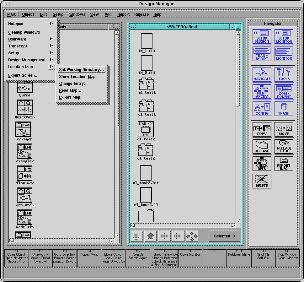
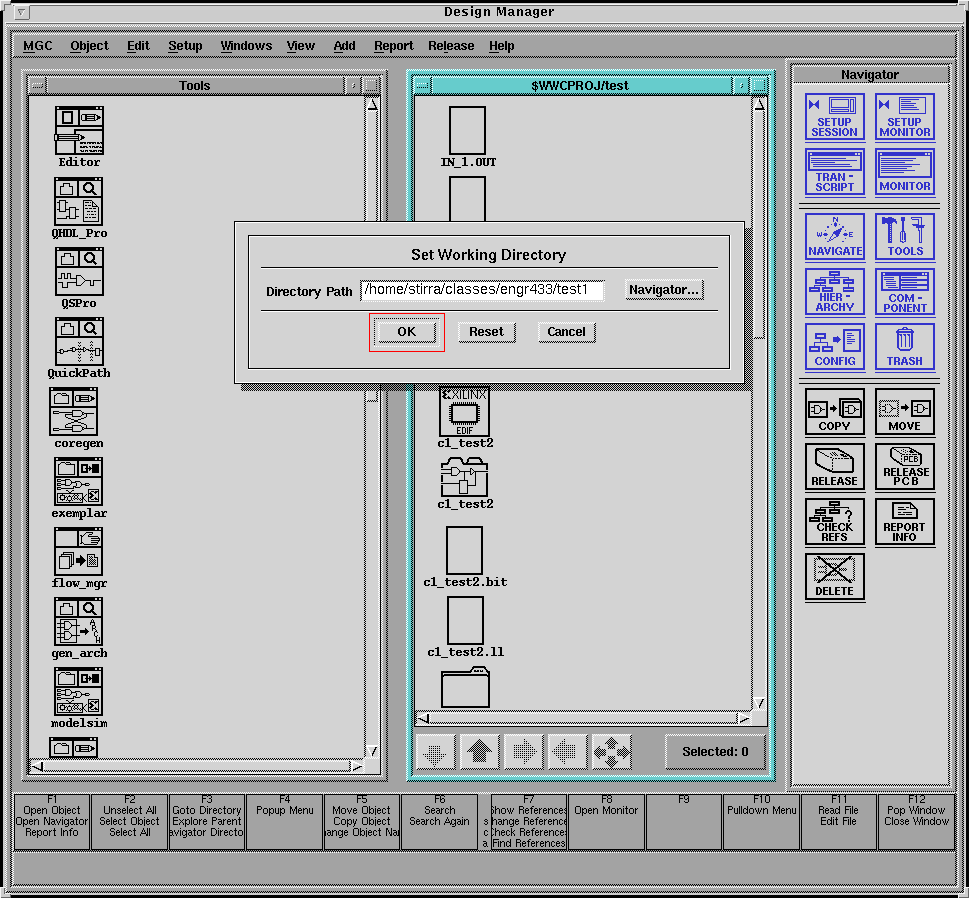
Before you run any tools, you should set your working directory. Inside Design Manager, select the File->Location Map->Set Working Directory drop down menu. Enter the top level of your design in the dialog box, in my case:
/home/stirra/classes/engr433/test1
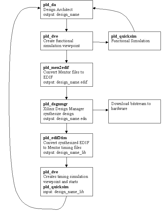
You may wish to look at a flowchart of the process of creating designs with the Mentor and Xilinx tools.
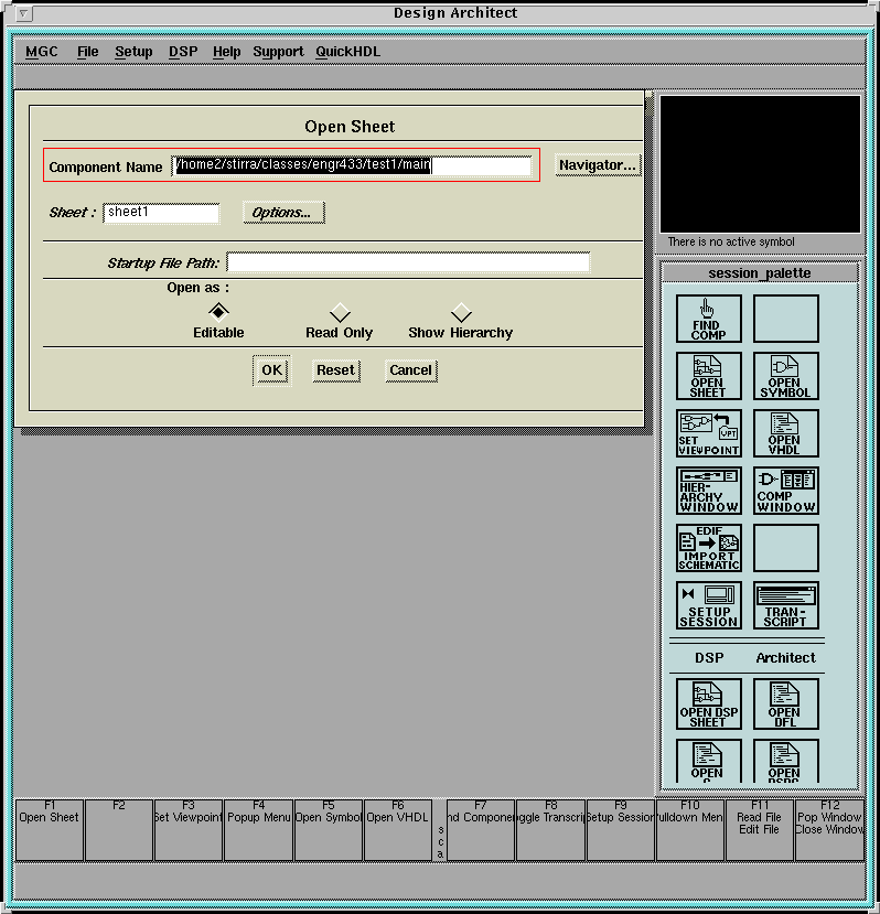
Double-click on the pld_da icon in Design Manager, and specify the name of your very top-level main schematic in the Design Architect startup dialog.
Select the Xilinx FPGA library palette from the library drop-down menu: Libraries->Xilinx, XC4000E, By Type.
Make this the default library by clicking on "set as default". You must not use any parts outside of the Xilinx library for this design. Using an FPGA as a part in a larger design will be covered in a different tutorial.
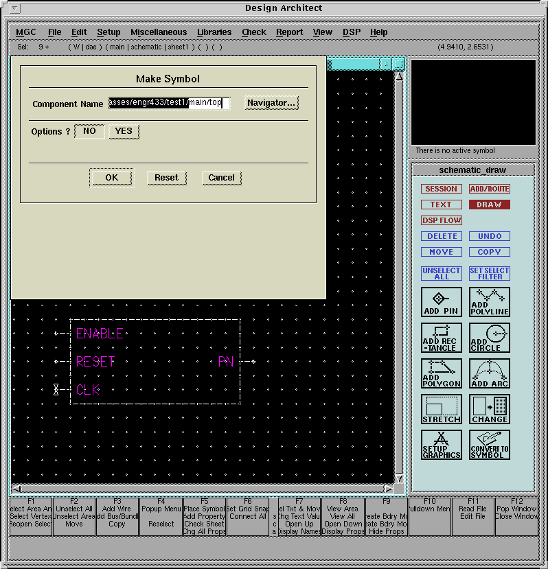
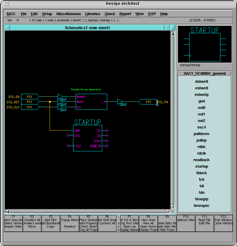
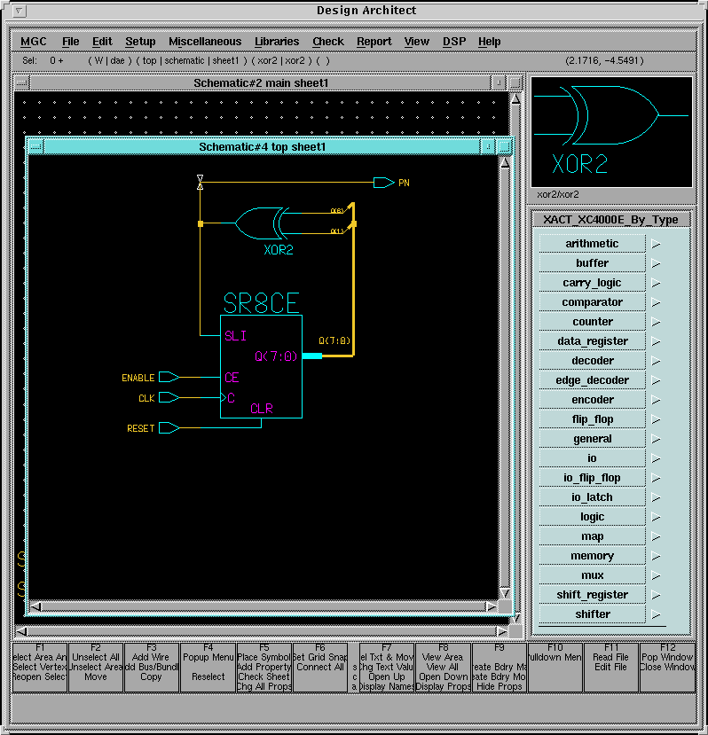
Every signal going into or leaving the FPGA must have an input, output, or bidirectional pad symbol (rather than a portin/portout/portbi symbol) at its end, and it must have a buffer wired to the pad (ibuf for input, obuf or obufe for output, or special clock buffer).
You may wish to specify the pin numbers on your schematic if you are going to be using your design with some existing hardware, where the pinout is fixed. Just edit the "PXX" PIN_NO properties in each of the ipad or opad symbols on your schematic.
If you wish to name signals pulled off of busses something other than the name of the bus with the signal number, use the "Setup Ripper" icon to change your ripper style to "Auto". If you use "Implicit", then it will automatically name your signal based on the bus name.
You must have a STARTUP block on your sheet, with the GSR (Global Set/Reset) tied to a reset input pin in order to properly simulate the design in QuickSim.
You can look at the datasheet for the XC4000E parts with acroread at: /home/common/datasheets/xc4000e.pdf.
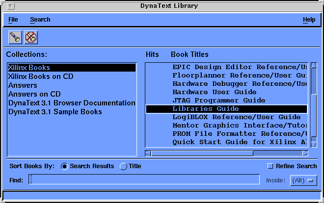
The Xilinx manuals, including the library reference, must be viewed with the DynaText browser tool, which is started with the command:
lassen:~/classes/engr433/test1> run_xilinx dtext
The "library reference" selection is the most useful book in DynaText.
Alternatively, you can the view the manuals and library reference or the datasheets on the Xilinx website.
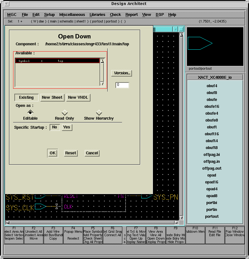
If you are doing a fairly large design, and wish to make it hierarchical, it is recommended that you put all the pads and buffers on the top level main schematic, and then you can use conventional (automatically created) portin and portout connectors for the lower-level sheets under each hierarchical symbol.
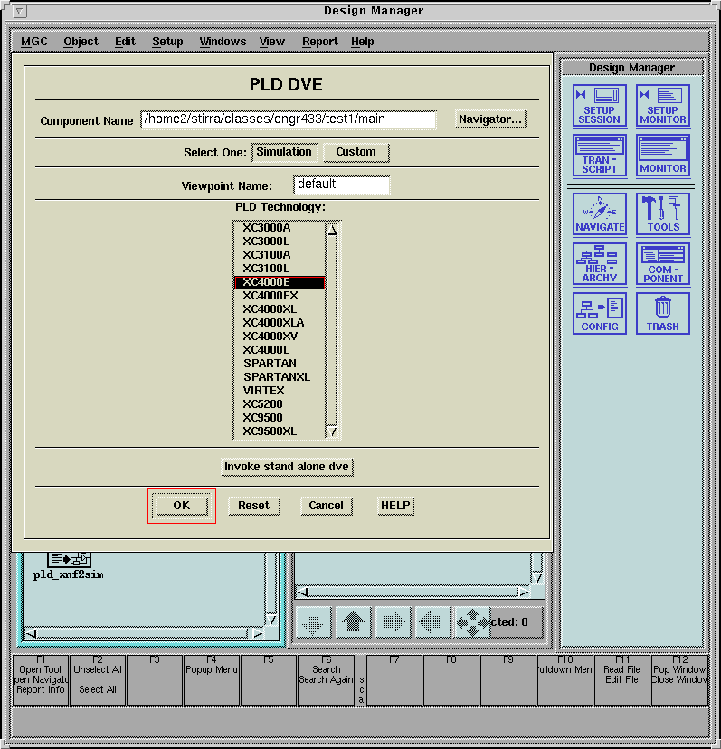
You now must generate a functional simulation viewpoint, using the Design Viewpoint Editor (pld_dve).
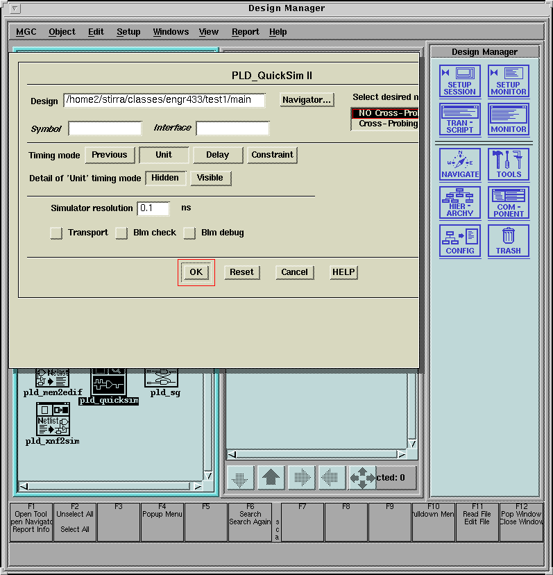
QuickSim (pld_quicksim) is used to perform the functional simulation. You can only use unit delay mode at this point, as no timing information is present in your design yet.
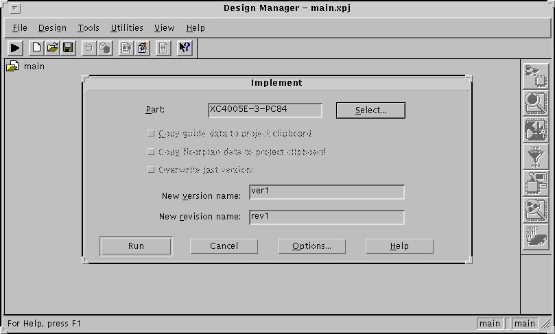
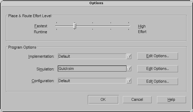
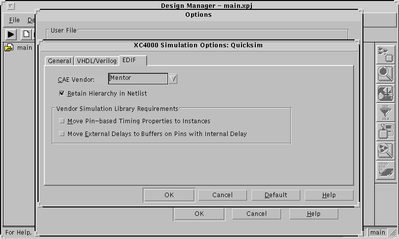
Within XDM you choose the Design -> Implement menu selection. You must select a part type, which is the XC4005E, PC84 package, -3 speed, for this class. You also must configure various options from the "Options..." subdialog. Check the "Produce Timing Simulation Data" box, set the Simulation template to "Quicksim", and edit the simulation template. Within the template, set the EDIF CAE Vendor to Mentor.
After OK'ing these option dialogs, you may proceed to "Run" the implementation. If you encounter errors, view the log file, make your corrections in DA, rerun pld_men2edif, and rerun the implementation. You do not need to exit either DA or XDM to update the design. You may either overwrite the existing version, or let it increment the version number.
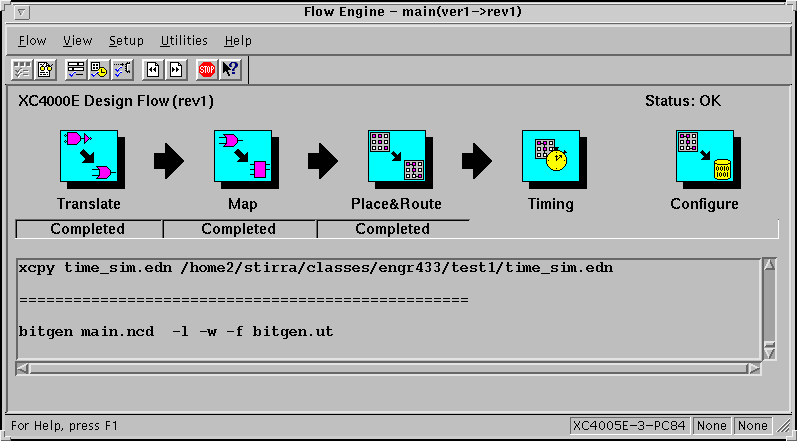
The "Flow Engine" gives you a graphical view of the progress of the mapping, placement, and routing steps of implementing your design.
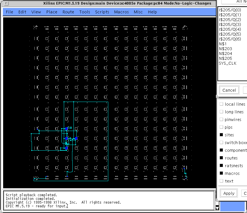
The Design Editor (Tools -> EPIC Design Editor) can be used to examine (and even modify) the finished implementation of your logic.
When you are finished, perform File -> Save Project, and exit the XDM.
Follow these directions carefully for successful timing simulation
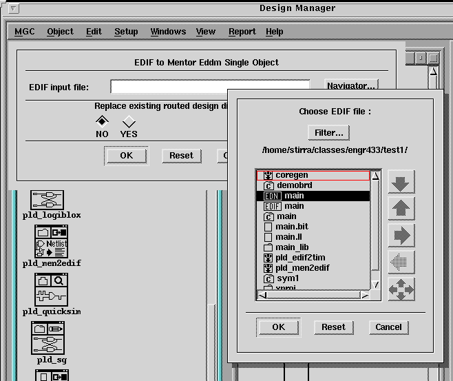
Use the pld_edif2tim program to convert the output of the Xilinx tools, with all timing information, back into a Mentor database for full timing simulation. The output EDIF file from the XDM flow engine has a ".edn" suffix, and is located in the top level of your design hierarchy. In my example, this will be /home/stirra/classes/engr433/test1/main.edn
If pld_edif2tim has errors, you probably forgot to set your working directory in the first step. Set it now in Design Manager and rerun pld_edif2tim.
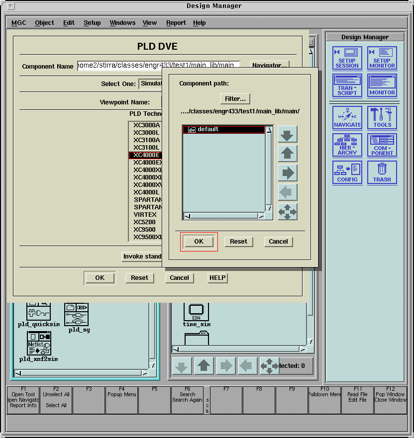
Run the pld_dve Design Viewpoint Editor again to create a viewpoint for the timing information. If your top level component was .../main, then you need to select the component .../main_lib/main as input for pld_dve. Use the default viewpoint under this component. The example design was: ~/classes/engr433/test1/main, so the component selected for DVE was: ~/classes/engr433/test1/main_lib/main.
Running QuickSim on the timing viewpoint is a little trickier than functional simulation. Both QuickSim and DVE come up for this process, and you select signals for tracing in DVE, not in QuickSim. Start QuickSim on the new component from the previous step (~/classes/engr433/test1/main_lib/main). Be sure to select "Cross Probing" this time. When DVE pops up, use the original design component (~/classes/engr433/test1/main) default viewpoint. DVE and QuickSim pop up in the exact same position, so you may not realize they are both running until you move the one on top.
Open the sheet in DVE, and select signals for tracing from that sheet. You can open down into your hierarchy by selecting the top level symbol, then using the pulldown menu File -> Open -> Down -> New.
To test your design on the FPGA Demo Board, you first must create the "bitstream" that will be downloaded to the FPGA. Do this by using the pulldown menu Tools -> PROM File Formatter in XDM. Now start the Hardware Debugger with Tools -> Hardware Debugger. This will only work if you are at a computer with a Demo Board and X-Checker cable attached.
Email me (Ralph Stirling) if you have problems or corrections to this tutorial.