Parasitic Extraction and Re-Simulation
Revised 4/27/2009
Objective
The goal of this lab is to take your D Flip-flop layout, extract the parasitic values from the layout, and re-simulate to see what effect these parasitics have on circuit performance.
Design Flow
The general design flow we are using is shown below. The portions we will do today are bolded.
Initial design
Capture the design as a schematic
Create a symbol of your design
Create viewpoints for downstream applications
Create a testbench circuit
Create a netlist for simulation
Simulate your design to verify operation
Layout a cell for this design (IC station)Verify layout
Check for layout rule violations (DRC)
Check layout against schematic (LVS)
Verify circuit operation
Extract parasitics and back annotate data base
Re-simulate
In this lab, you’ll complete the following steps:
Status check
View your D Flip-flop netlist
Open your layout and schematic
Extract your post-layout netlist
Simulate your new circuit using ADIT
Status
Check
At this point, you should have your schematic and layout completed for your D Flip-flop. You should have simulation waveforms that verify the correct logic operation of your circuit. You need to have the following two items precisely measured from your simulation:
Delay times (measured at the 50% level) for Clk to output low-to-high, and Clk to output high-to-low with no load on the output.
Rising and falling times (measured at 20%, 80%) for your output with no load.
It is imperative at this point that all of the following are completed satisfactorily with no errors. Carefully observe any warnings and point these out to the teacher or lab instructor for clarification:
Schematic check
Symbol check
Layout DRC passed
Layout LVS passed
Port labels placed on all your input and output signals, as well as VDD and GND
View Your D Flip-flop Netlist
Step 1: First, view the netlist created when you simulated your D Flip-flop in Lab#2. The netlist is located one directory below where you started Mentor Graphics. For example, if you named your D Flip-flop in Lab #2 dflop, your netlist filename will be dflop/dflop.src.net To view the contents of this file, at the Unix prompt type:
more dflop/dflop.src.net
Open your Layout and Schematic
Step 1: Navigate to the same directory you started Mentor Graphics from previously and open your D Flip-flop layout.
Step 2: Select Open from the Session palette, make sure the Edit button is selected, navigate to your D Flip-flop design, and click OK.
Step 3: Select the green ADK Edit button from the IC Palettes menu.
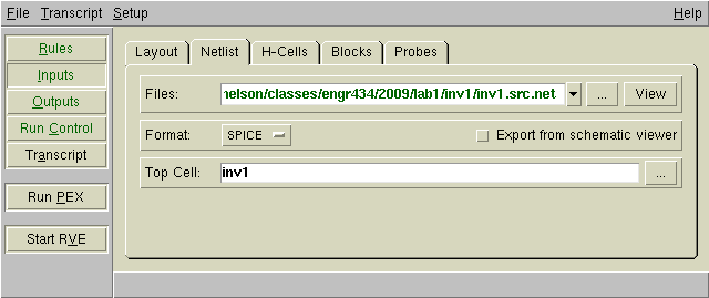
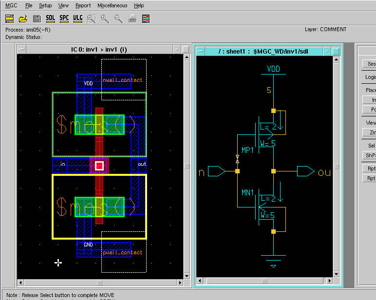
Step 4: Select the SDL > Open button from the ADK Edit palette to open the logic source. Mentor should now look like the following:
Note that an inverter is pictured above, and will be used as an example throughout this tutorial.
Extract Your Post Layout Netlist
Now that you have completed your layout and confirmed it is correct, it is time to extract the parasitic values from your actual layout. This will give you a spice netlist of your layout complete with one or all of the following options: resistance, parasitic capacitance, coupling capacitance, and inductance. For the extraction process you will use the tool Calibre Interactive – PEX.
Step 1: Make the layout window active and select Calibre > Run PEX from the top menu bar to start a Parasitic EXtraction. You will need to fill in a few screens to properly initialize Calibre. The Calibre setup information can be saved so you only need to enter it once. The Calibre extraction tool reads in your layout file and creates a Spice netlist suitable for simulation.,
Step 2: Calibre will start by popping up a Setup Calibre window. Fill in the Path to Calibre tree field with the following path and then select OK.
/apps/mentor/calibre-2008.2_33/ixl_cal_2008.2_33.26
Step 3: Next, Calibre will pop up the Load Runset File window. A Runset is setup information stored when you exit Calibre. Since this is your first time running Calibre, you don't yet have a runset file so click Cancel. Your screen should now look like the following:
Note
that any button that is Red
in Calibre
needs to be configured. Green
buttons have valid information (it may not be what you want, but at
least it is valid).
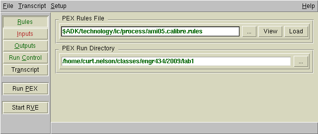
Step 4: Click the red Rules button in the upper left and set the rule file and working directory. The PEX Rules File box should be set to:
$ADK/technology/ic/process/ami05.calibre.rules
Your entry should be red as you type and turn green when you finish your entry, as shown below.
Step 5: Click the Load button. Nothing perceptable will happen, but that is OK.
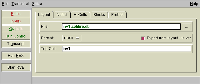
Step 6: Click the red Inputs button. Click on the Netlist tab and set the Files: box to:
$MGC_WD/<design>/<design>.src.net
where design is the name you assigned to your schematic. This entry points to the netlist that was created previously in Lab #2. For instance, if your design is named inv1, you would set this field to:
$MGC_WD/inv1/inv1.src.net
Your screen should now look like that shown below:
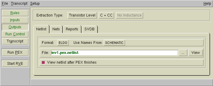
Step 7: Now, select the Outputs button on the left. At the top, the Extraction Type fields should be set as shown below. This will incorporate the parasitic capacitances into your spice file.
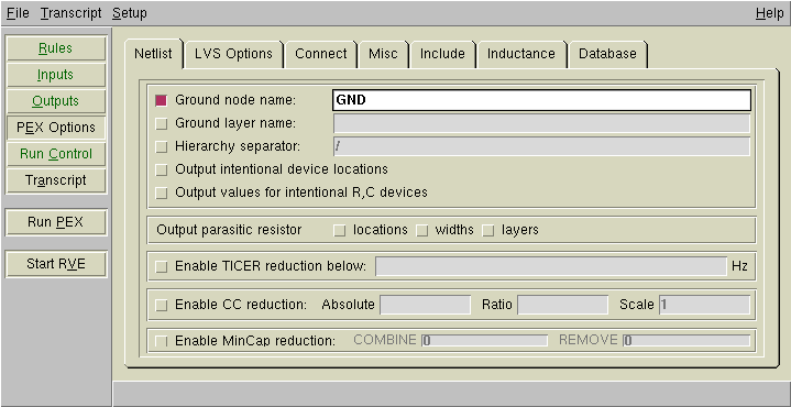
Step 8: Select Setup > PEX Options from the top menu bar. In the Netlist tab, click the Ground node name: check box and enter GND as shown.
Step 9: In the LVS Options tab, set the Recognize gates: check box to All. Also, make sure that VDD is one of the Power nets: and GND is one of the Ground nets:
Step 10: Select File > Save Runset As… and enter $MGC_WD/<design>.runset as the file name. For instance, using the dflop example, you would enter $MGC_WD/dflop.runset This saves your current configuration information. Click OK.
Step 11: You should now be ready to perform the extraction, so
click on the Run PEX. on the left. If a popup window
asks to overwrite the layout file, click OK. As each stage
completes, information will scroll through the transcript window.
If your extraction is successful, a new window will open displaying
the spice netlist created by Calibre. If you do not get
a netlist (this may take a few seconds) then review the transcript
window to locate problems and fix them. Your netlist should
look similar to: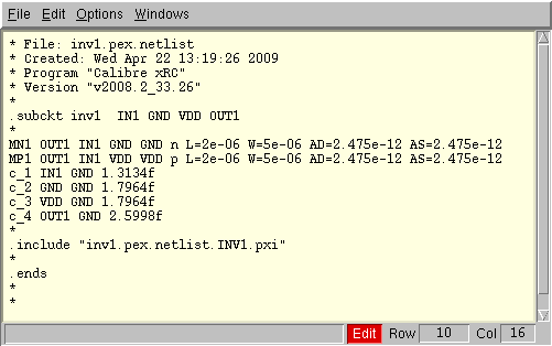
Notice that there may be up to two additional netlists which will be referenced via .include statements in the top level netlist (depending on the type of parameters you are extracting). The first will contain the RC networks and the second will contain the coupling capacitors. If the C (coupling capacitance) option was chosen, the top-level netlist will be the only one containing circuit specific parameters, and you should see a capacitance value from every circuit node to GND. Also notice that the the open window contains an Edit option which may prove to be useful for future simulations.
Step 12: Close the netlist window. Close Calibre PEX and save the runset if you wish. Exit IC Station.
T