Revised 4/28/2013
OBJECTIVE
The goal of this lab is to create a layout of the inverter that was designed and simulated in the first lab session, followed by a layout of your transmission gate and 2-input NAND gate.
INTRODUCTION
In Lab #1, you created a schematic of an inverter in DAIC and simulated it using ELDO and EZWave. You then created a symbol for use in later applications. In Lab #2, you created several subfunctions and used them to build and characterize a D Flip-flop. Today, you will first layout the design of your inverter with the Mentor tool called IC Station. Then, you will layout the designs of your transmission and 2-input NAND gates.
DESIGN FLOW
The general design flow we are using is shown below. The portions we will do today are bolded.
Initial design
Capture the design as a schematic
Simulate your design to verify operation
Create a symbol of your design
Create viewpoints for downstream applications
Create a netlist
Layout a cell for this design (IC station)
Verify layout
Check for layout rule violations (DRC)
Check layout against schematic (LVS)
Verify circuit operation including layout parasitics
Extract parasitics and back annotate the design
Re-simulate
In this section, you will complete the following steps:
Invoke IC Station
Set up tiling
Create a new schematic driven layout
Setup layout display dynamics
Place devices from schematic to layout
Show all levels of hierarchy
Place and edit a path
Perform a Design Rule Check (DRC)
Add port labels
Check the Layout Versus the Schematic (LVS)
For future use
0 Create circuit
Create a directory for this lab
Make sure that this new directory becomes the current directory by using the cd command.
Use DAIC to create an inverter schematic and its symbol. Follow the instructions used for Lab1. Set up for simulation, run the simulator and see pretty waveforms, but don't do the measurements that we did in Lab 1.
1
Invoke IC Station
You are going to use one of the advanced features of ICStation within the Mentor environment to have the schematic of the inverter gate help generate the layout. This function is called SDL - Schematic Driven Layout. The layout functions within the Mentor environment (along with the ADK design kit support) will help us to automatically create the transistors via a device generator, and to track the wiring of the cell so that it matches the schematic we originally created. In the end, we can check the layout to see if in fact, it still matches the schematic. This function is called LVS - Layout Vs. Schematic.
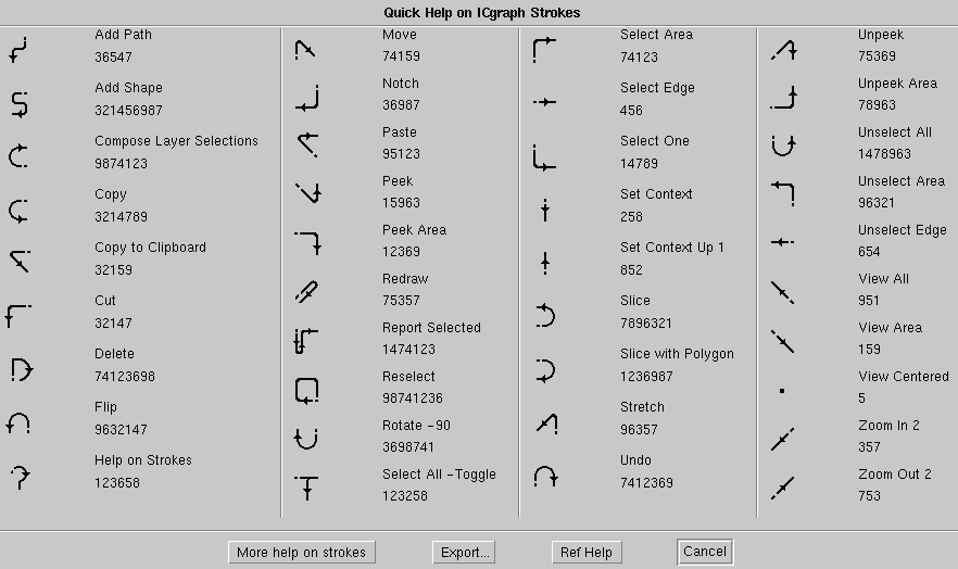
Unfortunately, Mentor Graphics is not consistant with the use of strokes across their tool set. The strokes in IC Station are shown below and differ somewhat from DAIC.

1.1 If DAIC is open, close it.
1.2 Navigate to your Engr434 lab 3 directory if you aren't already there. This should be ~engr434/lab3 or something similar. Start the mentor script that sets up the environment for layout by typing the command ic at the command prompt.
2 Set Up Tiling
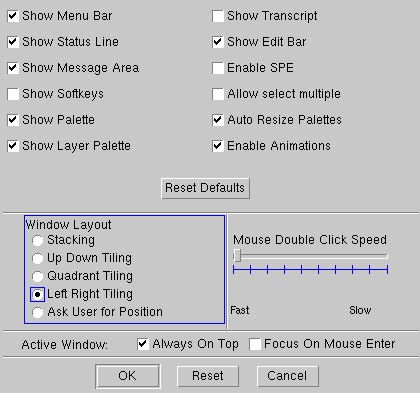
The first step is to setup the display with Left-Right Tiling so you will have a layout view and a schematic view of the design, side by side.
2.1 Click Setup > Session… in the menu bar and select the Left Right Tiling button on the Window Layout section as shown below. Leave the other options as they are and click OK. This will setup the display with two views, a schematic view and a layout view when you open your design.
3 Create a New Schematic Driven Layout
3.1 Click the Create button in the Session palette to create a Schematic Driven Layout. Your screen should show this:
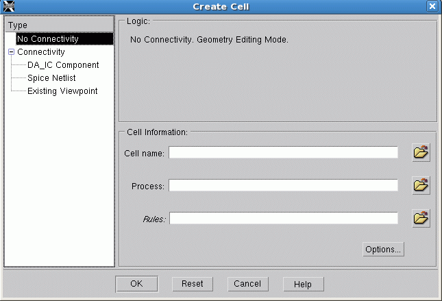
In the Type field at left, click on Existing Viewpoint. You should see this:
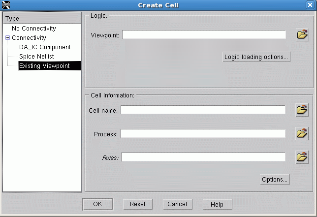
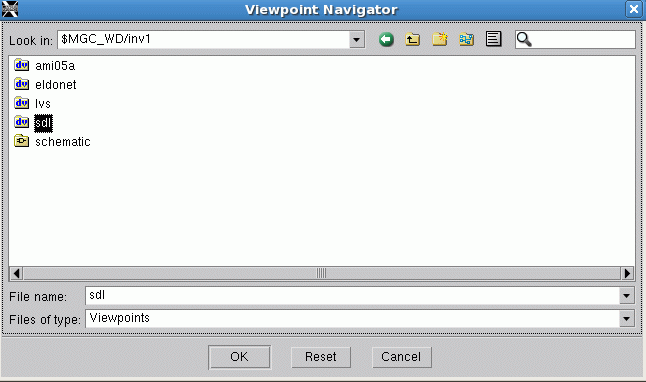
3.2 In the Viewpoint field, click the Browse symbol, double-click the inv1 component in the window that opens, and then click on the sdl viewpoint as shown below. Note that this is a “viewpoint" of the inverter you created in the first lab. Your screen should look like the following:
3.3 Click OK to return to the Create Cell screen. In the Cell Name field type in $MGC_WD/inv1 (where inv1 should be the name of your design, usually the same name as your component, i.e. the schematic).
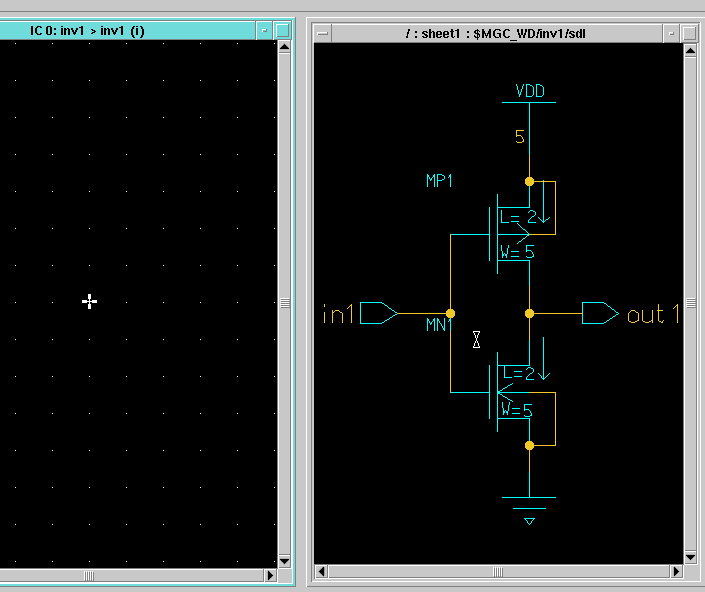
Leave the other fields as they are and click OK. IC Station will create a tiled window view as shown below, with a blank layout window on the left and a schematic window on the right showing a schematic of your inverter.
4
Show the Layer Palette
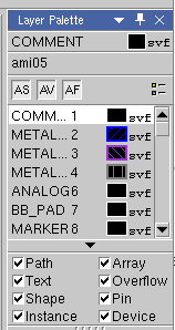
The layer palette should be visible in the upper right portion of the IC Station window as seen below. If it is visible, go on to section 5. If not, follow steps 1-4 below.
Step
1: Select Other > Layers > Show Layer Palette… from
the menu bar. This will open the Show Layer Palette
dialog box where you can select the layers you want to show.
Step 2: Select layers COMMENT through METAL5_BLKG by left-clicking on COMMENT, then left-clicking on the scroll-down bar on the right of the Show Layer Palette window until you see METAL5_BLKG (layer number 164).
Step 3: Press the Shift key, and while holding it down, left-click on METAL5_BLKG. The layers above and including layer 164 should be highlighted.
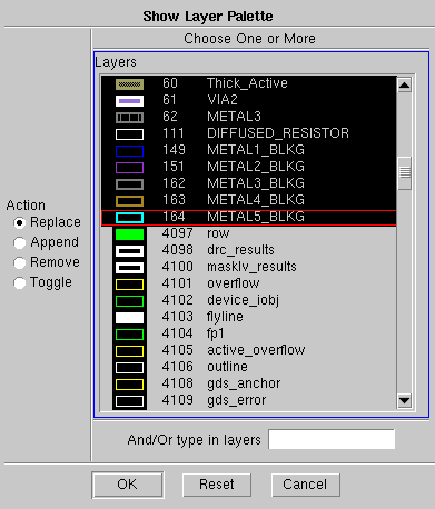
Step 4: Click OK. IC Station will now include a Layer Palette in the top right hand corner of the screen.
5 Set Up Layout Display Dynamics
Step 1: Make sure the layout window is selected by left-clicking on the title bar. Click Setup > Dynamics: in the menu bar to open the Setup IC Dynamics window like this:
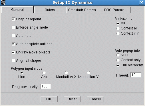
Under the General tab set:
Redraw Level: All
Auto Popup Info: Full Hierarchy
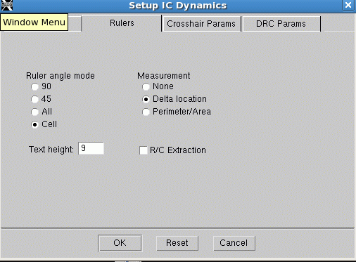
No changes to the ruler screen.
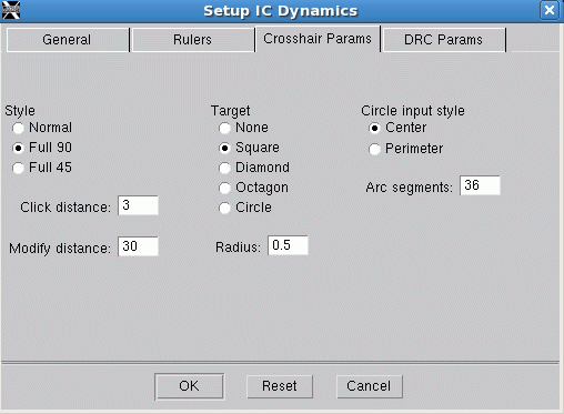
On the Crosshair screen, set
Crosshair Parameters Style: Full 90
Crosshair Parameters Target: Square with Radius 0.5
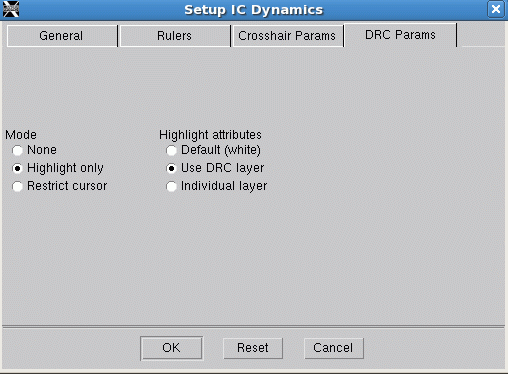
OTF Drc Parameters Mode: Highlight Only
OTF Drc Parameters Highlight Attributes: Use DRC Layer
Leave all other fields as they are and click OK to accept the changes and close the dialog box.
Step 2: To save your setup information click Setup > Save Setup from the menu bar and your preferences will be saved. Now, each time you start IC Station, the setup configuration you just saved will be automatically loaded.
Note: If you exit your design and wish to reopen it, you will need to reopen the logic portion of your design. Open your project, then select File > Open > Logic. The logic will open in the right pane.
6 Place Devices from Schematic to Layout
Step 1: Be sure that your layout pane is selected by left-clicking on it. Click on the green ADK Edit button near the bottom of the IC Palettes menu. You may need to scroll down to the bottom of the menu list if it is not visible (use the mouse scroll wheel or the page down/up buttons). The ADK Edit menu should appear as follows:

Step 2: From the ADK Edit palette, click on the SDL Place> AutoInst button which will automatically place the transistors from your schematic into the layout edit window on the left. When it is finished, if needed, press Shift F8 to cause the whole layout to be seen. You should see both of your MOS devices connected by two skinny, vertical yellow lines. These lines are called “overflows” and indicate the connections that should be made between devices.
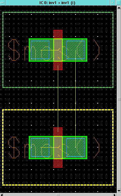
The layout on the left of your screen is often referred to as a cell. The next step is to determine the approximate boundaries of your cell and place layout port symbols there. Layout ports are used as interconnections between cells, because larger designs are built from the bottom-up by interconnecting groups of cells together. I have coined the term layout port here to distinguish ports used on the schematic from those used in the layout. Both serve a similar function, namely to identify a connection point, one between schematics and the other between cells in the physical layout.
Step 3: Before placing ports, you must define a port style. Click Setup > SDL… on the menu bar. In the Setup SDL pop up window, find the Setup Values sub-window. Select the SDL Port Styles option as shown below:
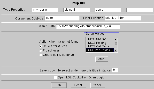
and then click the Setup… button right below it.
Step 4: A Set Active Port Style window will open. In the Select Attributes from… area, click on the Process Ports button. In the Select a Port Style area, click on the port (width = 4) option as shown below:
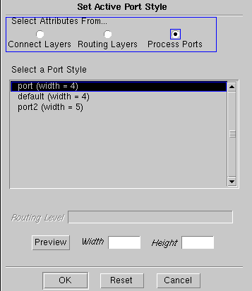
Leave other options as they are and click OK. Click OK again to close the Setup SDL window.
Step 5: Next, you need to physically place your ports on your layout. In the ADK Edit palette, click on the SDL > Port button, just to the right of the AutoInst button. One of the ports (probably VDD but possibly Gnd) on your schematic will be highlighted in green. In the layout window, you will see a white rubber-band line that indicates the corresponding section of the layout that needs to be physically tied to the port. Next, you need to set the layer and dimensions of this port. In the lower left of your screen, click on the Options tab in the PLA PO S popup window:

Select layer #2 (METAL1.PORT), and set the width and length both to 4. Note that you must first select the Layer, and then the dimensions or the dimensions will default back to 1,1. This establishes which layer you are going to create the port connections on and the size of the connection pad. Click OK to save these selections.
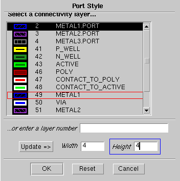
Step 6: Now, when you move the cursor over the layout you will see a pair of white crosshairs with a blue square attached. The blue square will be labeled with the layer, METAL1.PORT, and the port name, VDD, from the schematic. Move the cursor so that the blue square abuts the top boundary of your cell, and is lined up directly above the highlighted white square on the layout as shown below.
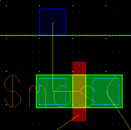
Place this layout port by left-clicking. You should now see a diagonal-hatched blue square, with a yellow wire attached to what was previously the white square in the layout. Note that you have placed your port where it will be convenient to route a wire from it to the proper place on the layout at a later time. Note that during this placement process, you can use strokes to zoom in or out on the screen, and also just a middle-mouse button click is helpful to reposition the center of the screen.
Step 7: After placing the first layout port, another schematic port will be highlighted (probably GND). Note that the highlighted square this time is located in the lower section (NMOS) of the layout. Verify that the layer is METAL1.PORT and the dimensions are the same as the VDD port pad. If they are not, select the Options button again and reenter the proper values. Abut this port against the lower edge of the cell and directly below the white highlighted rectangle as shown below. Note that these ports can be moved later if you misplace them (see step 9).
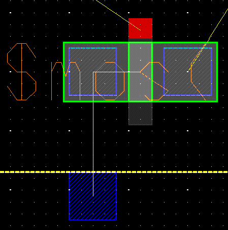
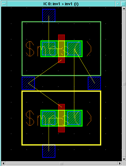
Step 8: Finally, place the in and out ports vertically midway between the two wells, so that the left edge of the in port lines up with the left edges of the wells, and the right edge of the out port lines up with the right edges of the wells. Your final layout should look similar to that shown below. Note that in general, there will always be a layout port for VDD, one for GND, and one for each Portin or Portout shown on the schematic.
Step 9: If you misplaced any ports, you can move them now. Left-click on the port you wish to move to highlight it. Then type v (a popup box will automatically appear) and type Return. Left-click to place the port in the desired location.
Step 10: Unselect everything in the layout window by using a left-to-right U stroke or press F2.
Step 11: The next step is to place substrate contacts. Each N channel MOSFET should have a contact from GND to the substrate near the MOSFET. Each P channel MOSFET should have a contact from VDD to the substrate (or at least one contact for every 4 to 5 transistors). These substrate contacts, also called tub ties, consist of a diffusion square with a select box around it, a via, and a square of layer metal1. Connection is made from metal1 to the substrate. First, you will place the nwell contact.
Type nwc (which stands for nwell contact, and brings up a text box) and then press Return. Position the cursor horizontally so that the right-hand side of the nwell contact outline borders the right-hand side of the nwell (top) outline. Position the cursor vertically so that the nwell contact sits above the nwell, and the bottom of the nwell contact is two cursor units (note the cursor resolution is 0.5 microns) as shown below.
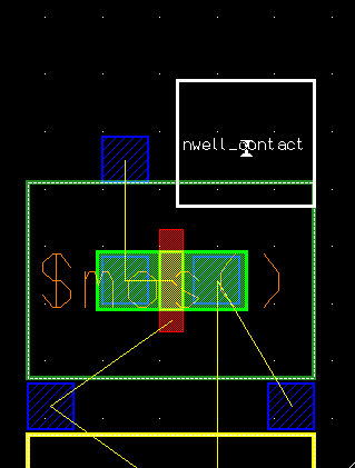
Left-click to place the nwell contact.
Step 12: Type pwc to place the pwell contact. Type Return and position the cursor horizontally in the same place as you did the nwell contact. Move the cursor down and place the pwell contact in a mirror position to that of the nwell contact. Left-click to place the pwell contact. Unselect everything and when you are finished, your layout should look like that below:
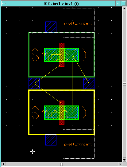
For your inverter, you only need one pwell and one nwell contact. For larger cells, you will likely need more.
7 Show All Levels of Hierarchy
Step 1: Your layout actually has some hidden layers, primarily in the pwell and nwell contacts. To see all layers of the hierarchy, zoom out in the layout window until you can draw a rectangle around the entire design. Select everything by left-clicking, holding, and dragging a rectangle around your design. From the menu, select Context > Hierarchy > Peek: and enter 4 in the Number of Levels window that pops up.
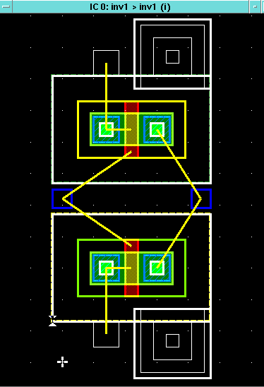
Click OK, unselect everything, and all layers should now be visible.
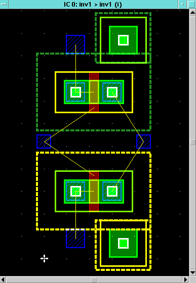
8 Place and Edit a Path
After you have placed the well contacts, wires need to be placed between transistor terminals and ports. Paths are used to create metal1, metal2, and poly connecting wires.
Step 1: Start path add mode using one of the methods below:
1)
Hold down the right mouse button with the cursor positioned over the
layout and select Add
> Path:
2)
Use a stroke (draw a question mark with a stroke to see the stroke
options)
3)
From the menu bar select Objects
> Add > Path:
4)
From the ADK
Edit palette,
select Add
> Path*
In all cases, a small pop up ADD PA box will appear at the lower left.
Step 2: Before placing a path, you need to set some options. Left-click on the Options… box. This will open a larger set up window. In the width field, enter 4. This sets the width of the path, in units of microns.
Step 3: Scroll down in the Choose one layer name window and select METAL1 (layer #49). Alternatively, you can type the layer name in the window below the choices.
Step 4: Left-click on the Keep Options Settings check box so that the next time Add > Path is invoked the same layer and width will be selected. Your configuration window should appear as shown below:
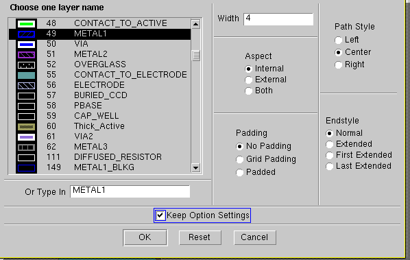
Leave the other options as they are and click OK to close the dialog box.
Note that when routing METAL1 to the ports, each port needs to be completely covered with the wire. That is, a wire can be wider, but not narrower, than the port that it covers.
Step 5: Move the cursor to the path starting location (the left side of the pmos device) and left-click. Move the cursor to the ending location (the VDD port) and left-double-click. It will take some practice to get it lined up correctly. If you are off, select the wire, delete it, and try again. See the blue rectangle below.
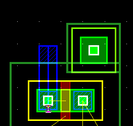
Step 6: Continue adding paths until all wiring is complete. You will need to add paths of layer METAL1 between each of the following:
The
left side of the pmos device and the VDD
port
The right side
of the pmos device to the output port
The
output port to the right side of the NMOS device
The
left side of the nmos device to GND
The nwell
contact to VDD
The pwell
contact to GND
The input port
to the device gates
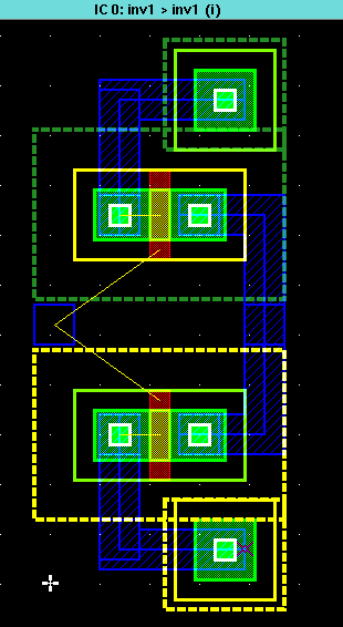
When you are finished (except for the last item), unselect everything and your layout should look like that shown below:
Step 7: The last path to place is the poly connection between the gates of the two devices. Start path-add mode if you are not still in it and select the Options… button in the popup box. Select the POLY layer (layer 46) and change the Width to 2.
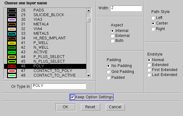
Click OK. Route the wire between the two device gates now, making sure to overlap by at least 1 micron.

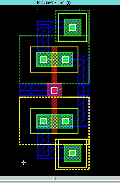
Step 8: You now need to place a contact between the poly and metal1 layers, so that a connection can be made from the input port to the gates of the devices. Position the cursor at the center of the intersection point, type pc, and press Return. A script will run and place a stack of layers that make up a poly contact (poly, polycontact, and metal1).
Step 9: Your last path to add is that between the input port and your poly contact. Do so now, unselect everything, and your final layout should look like the following:
9 Perform a Design Rule Check (DRC)
Step 1: From the ADK Edit palette, select Verification > Drc > Check. Note: you must click on the right-facing arrow to the right of the Drc entry in the Verification portion of the ADK Edit palette. When a menu pops up, select the Check option. This will bring up a CHE DR menu box in the lower left portion of your screen. Left-click on OK to perform a DRC check on your entire layout. It is also possible to perform the DRC on just a portion of your layout by left-clicking and dragging the mouse over the desired area.
At the bottom of the layout window, a message will be displayed summarizing the results:

If Total Results = 0, then you have no design rules violations. A result means that a rule violation was found.
Step 2: To view the errors one at a time, select Verification > Drc > First to see the first violation. The cause of the violation will be highlighted in white on the layout and there will be a description of the violation which appears in the status area at the bottom of the window. Select Verification > Drc > Next to step through the DRC errors currently in the results database. Verification > Drc > Delete All will clear all DRC errors from the results database. As you are checking, you can fix errors and continue showing the next one. Keep in mind that errors in nearby structures might be fixed with one change, so it is wise to rerun the DRC after every few fixes.
10 Add Port Labels
Step 1: Once all DRC violations are fixed, select Connectivity > Port > Add Text On Ports: from the menu bar. Enter METAL1.PORT in both the Shape layer and Text layer boxes.
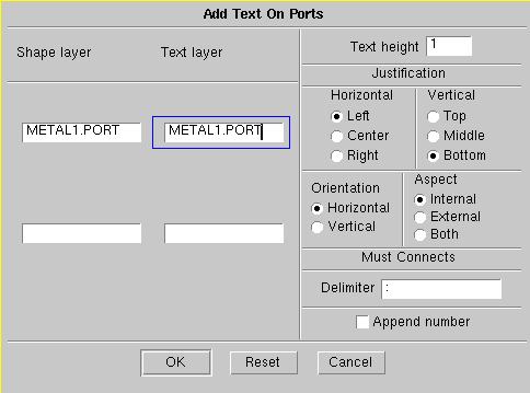
Leave all other options as they are and click OK. This will automatically add text to all the ports in your design. Note that the port text is used by the downstream application Calibre to identify the ports in your design. Without the text, the extracted netlist would be useless.
11 Check the Layout Versus the Schematic (LVS)
LVS is used to check that your layout corresponds to your schematic. This is another way to verify that your layout is correct by creating a netlist based on the layout geometry and comparing it with the original schematic netlist. They should be the same.
Step 1: First, close your logic window by selecting SDL > Logic > Close from the ADK Edit palette.
Step 2: From the ADK Edit palette, click on the Verification > LVS button which brings up the LVS (Mask) dialog box. Under the box titled Source Name, left click on Browse, double-click on the inv1 component, and single-click on the lvs viewpoint. Click OK to close the Viewpoint Navigator window and your screen should look like the following:
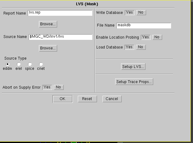
Step 3: Click the Setup LVS… button and add GND to the row of Ground names as shown below:
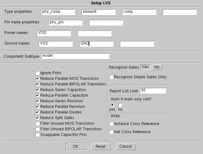
Click OK to close the window.
Step 4: No other changes need to be made in the LVS (Mask) dialog box, so click OK and the Layout-vs-Schematic check will now be run.
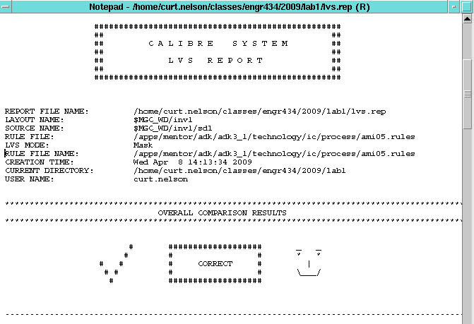
Step 5: To view results, select Report > LVS next to the LVS item on the ADK Edit palette. If you see a checkmark, a smiley face, and a “Correct” box as shown below, then you have a good layout! If not, read the report to see what types of problems exist. Note that LVS problems can be challenging to track down, but resolving them is essential to ensure a proper layout.
Step 6: You can print the LVS report by using File > Print > Print Document: on the menu bar and specifying sun-lab as the printer name. Note that the report is also written to a file (as specified in the LVS dialog box), so you could open the file with an editor and print only part of the report if desired. Note that by default, LVS uses the same report file name each time, thereby overwriting any other LVS report previously created in the directory from which IC Station was started from.
Close the report by right- or left-clicking the little box in the upper left corner of the LVS report window and selecting Close.
12 For Future Use
The following three cases may come in handy at some future point in this course. You need not complete them at this time.
Case 1: To connect the metal1 layer to the metal2 layer, use a via. A via is created by drawing a 2x2 lambda box of type VIA over the intersection of the metal1 and metal2 layers. To place this via, select Objects > Add > Via > Active Via In the pop-up window, choose the via option (not via2) and click OK. Choose the location you want and left-click to place the via.
Case 2: Ports that you add, default to a layer type called METAL1.PORT. If you wish to change the port to a different layer (you don’t right now), you can change the port type as follows:
1) Select the port (or ports) that need to be changed. You likely will need to change the select filter so that only the port (which is a shape) is selected and not the path (i.e. wire) that covers it. On the menu bar choose Select > Setup Filter. A large pop up box allows selection of object types to be selected. Make the necessary selections, and click OK.
2) From the menu bar, select Objects > Change Layer A pop up box will open. Click the desired layer, i.e. METAL1.PORT (or type in its name), and click OK. The selected ports will be changed to the newly specified type. Meta11 ports will be the same color as metal1, just like Metal2 ports are the same color as metal2. This can be a bit confusing when looking at the layout.
Case 3: If you are creating a standard cell style layout, type pr and press Return. This will place VDD and GND rails with ports and the corresponding NWELL and PWELL layers. The lower left corner of the GND rail will be at location (0,0).
Step 1: Make a color print of your layout by printing to the color printer using lws-cp3505 as the printer name. Write down the dimensions (in microns) of your layout, on your layout.
Step 2: Save your inverter layout by selecting from the top menu bar File > Cell > Save Cell
Step 3: Exit IC Station and grab a cold lemonade.
The following information is due at the beginning of the first class period following this lab. Staple the following items together in the order presented below.
A printout of your LVS report files.
Schematic diagram of your circuits.
A color printout of your layouts, annotated with dimensions.
Developed by Curt Nelson. Revisions and updates by L.Aamodt