Creating a Schematic with Design Architect and Performing a DC Analysis with Accusim


1. Create a schematic of a simple resistive ladder network with Design Architect
 
1.1 You should make a habit of using the Unix directory structure to manage your files (just as you use folders in Windows for the same purpose). You should create a directory under your home for each  class and keep all of your work for that class in that directory. You should also create directories under each class directory for each category of work such as "tutorial, "labs," "design_project'" etc.:
>> mkdir engr357
>> cd engr357
>> mkdir tutorials
>> cd tutorials
>> mkdir lab1
>> cd lab1
Don't forget to go back into this directory before you resume work if you logout and log back in at a later time...

1.2 Start the Design Architect tool (DA) to construct the schematic of the circuit:

>> run_en2k da

A new DA window should appear:

Note that when the tutorial refers to a "palette", it means the area to the right that is currently labeled session_palette. Also, when the term "menu item" is used, it refers to the menus at the top of theDA window.

1.3 Create a new component for the design called circuit1. Click on the  button in the session_palette to bring up the Open Sheet dialog box.  Place the cursor at the end of the Component Name item and click the left mouse button (LMB).  Type "/circuit1" without moving the cursor from that box. The result should be an Open Sheet dialog box like the one below:

If you make a mistake typing, use the backspace key, not thedelete key to erase the incorrect characters. In the Mentor tools, the delete key will erase all of the highlighted characters, so you must be careful to not press the delete key unintentionally. If this happens, it is easiest to simply click the Cancel button and open the dialog box again.

When creating a new component in the Mentor tools, DO NOT CHANGE THE SHEET NAME FROM THE DEFAULTsheet1. Changing the Sheetname has some undesirable consequences for novice users, so it is best to leave it as sheet1.

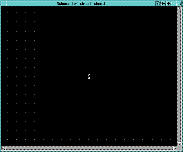
When the Open Sheet dialog box looks like the one above, click OK. A new schematic window labeled circuit1 like the one below should appear:

1.4 Use the Libraries->MGC Analog Libraries item to bring up the MGC Analog Libraries palette. Click on the Generic Parts item in the palette and then on the RESIST item. When you do this, a version of the resistor symbol will appear in the active component window above the palette. A ghost image of the resistor will appear in the schematic window when you move the cursor over it as shown below.

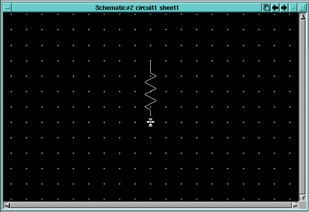
Place the cursor near the left side of the schematic window and click the LMB. This will place the resistor component in the schematic window.

1.5 Click on the RESIST-H symbol and place a horizontal resistor next to the one you previously placed. Alternate between placing the two types of resistor until you have a schematic like the one below:

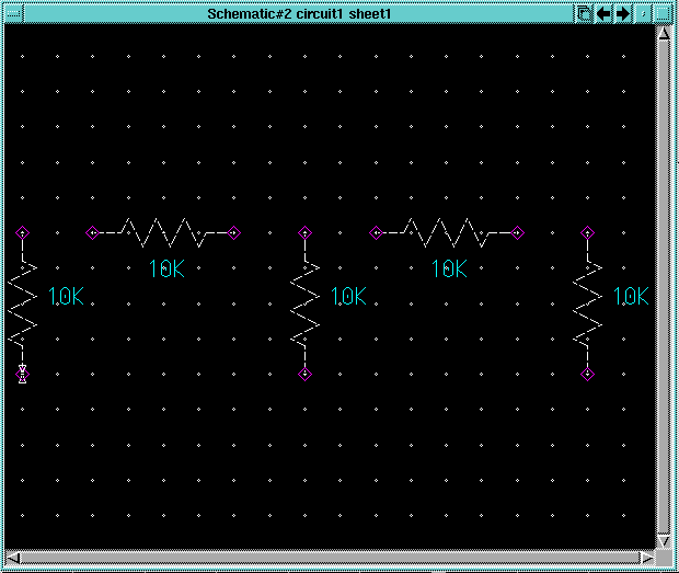
Note that you may have to use the View->Zoom Out menu item to give you more area to place the components and the View->All menu item to zoom back in to see the same view as above.

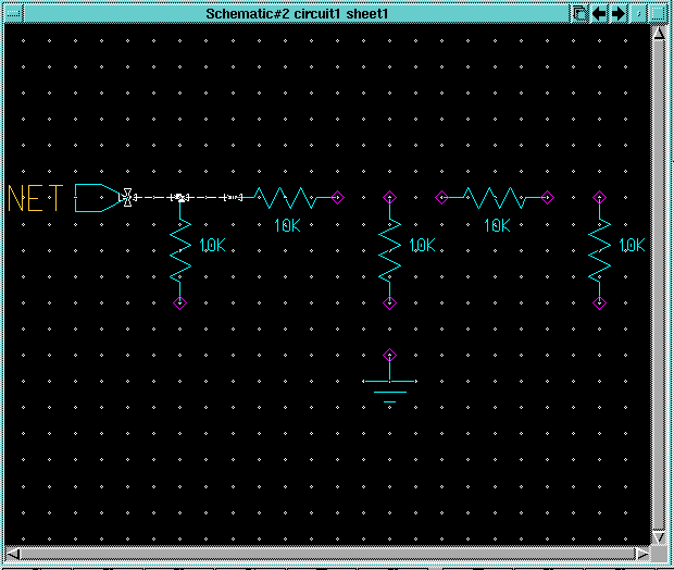
1.6 Place a PORTIN component to the left of the resistor network and a GROUND component under the resistor network like this:

1.7 Place the cursor in the schematic window and click and hold the right mouse button (RMB). This will cause a pop-up menu to appear. These pop-up menus are context sensitive in that they change based on which type of component in the schematic is selected (highlighted in white). Move the cursor down over the Unselect item and move the cursor to the right. A cascading menu will appear. Move the cursor over the Allitem and release the RMB. All of the components in the schematic will be unselected. You can also unselect all components by pressing the F2key on the top row of the keyboard. The Mentor tools frequently give you multiple ways to perform common actions like this.

1.8 Place the cursor in the palette area and press the RMB. Select the Display Schematic Palette item and release the RMB. The schematic_add_route palette will appear. Press the button. A small Add Wire dialog box will appear at the bottom of the DA window and the cursor will change to a cross hair within the schematic window. Place the cursor over the pin of the PORTINcomponent and click the LMB.  Move the cursor to the top pin of the resistor to the right and single click the LMB. Move the cursor to the pin on the next resistor to the right and double click the 
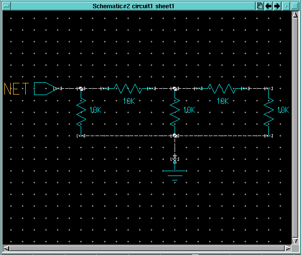
LMB to end the wire. The result should be a single wire like this:

1.9 Add the remaining wires in a similar manner so that schematic looks like this:

Click Cancel in the Add Wire dialog box to exit the wiring mode and hit the F2 key to unselect all of the wires.

1.10 Now you will change the resistor values and name the input port. Place the cursor in the schematic window and click and hold the RMB. Move to the Select Area->Property item and release the RMB.  Use the LMB to draw a box around the word NET on the schematic. Use the RMB again to bring up the pop-up menu and select the Change Values: item. In the small dialog box that appears, place the cursor in the New Value item and type "in1". Click OK in the dialog box.

You could have performed the same action without going through all of the above steps by simply placing the cursor over the word NET and hitting the shift key and the F7 key simultaneously. This would have selected the property and brought up the dialog box.

1.11 Use one of the above mechanisms to change the resistor values to the values shown below:

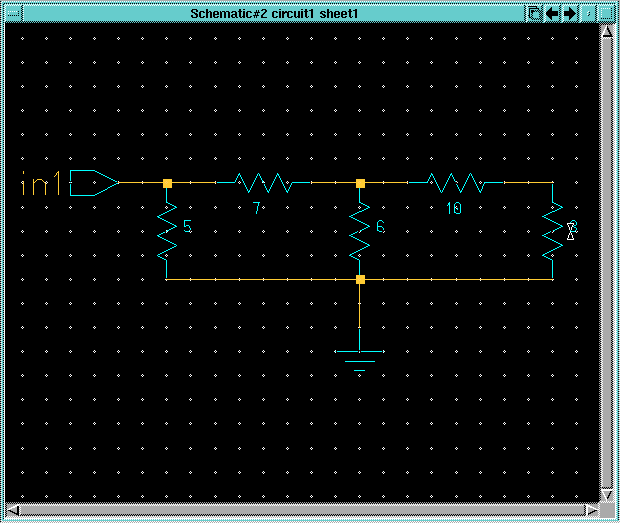
1.12 Now you will name the nets in the schematic so that they are easier to identify in the simulation. This is not strictly necessary, especially in a small schematic like the one you are building, but it is a good habit that will help debug complex designs. Place the cursor right on top of the place where the wires cross in the middle of the circuit - above the 6 ohm resistor - and click the LMB. This should result in only the crossing point (the vertex as its called) being selected. Use the RMB to bring up the pop-up menu and select the Name Nets: item. Place the cursor in the Property Value item in the dialog box that comes up and type "net1" and hit Return. Move cursor into the schematic window and you will see a ghost image of the "net1" name following it. Place the cursor above the selected vertex and click the LMB to place the name.

Use the same mechanism to assign the name "net2" to the wire between the 10 ohm and 3 ohm resistor. Note that the wire attached to the PORTIN already has the name "in1" from the PORTIN and the one remaining net does not really need a name because it is connected to the ground component and will be called GND in the simulation.

1.13 Use the Check->Sheet menu item to check the sheet. The Checkwindow that come up should say "circuit1/schematic/sheet1" passed check : 0 Errors, 0 Warnings at the bottom. Close the Check window.

1.14 Use the File->Save Sheet menu item to save the schematic sheet and then close the schematic window and close DA.
 

2. Create a simulation viewpoint using Design Viewpoint Editor
 
When you create a schematic using Design Architect, DAhas no idea what you are going to use the schematic for, digital simulation, analog simulation, VLSI layout, etc. Before the schematic can be used for a specific purpose, a design viewpoint must be created for it. A viewpoint tells the down-stream tool (the tool that uses the schematic after it is created with DA) what information on the schematic is to be used and what properties on the instances contain the information. Some tools like the digital simulator Quicksim II, create the design viewpoint automatically if it does not exist, but Accusim does not, so we will create it explicitly using the Design Viewpoint Editor (DVE)

2.1 Open DVE on your circuit1 design:

>> run_en2k dve circuit1
2.2 Use the Setup->Accusim menu item to setup the viewpoint for Accusim.

2.3 Use the File->Save Design Viewpoint menu item to save the viewpoint and exit DVE. Note that you will nothave to redo the viewpoint if you change the schematic using DA.
 

3. Simulate your schematic using Accusim
 
3.1 Start the Accusim simulator on your circuit1 design:
>> run_en2k accusim circuit1
You will see an Accusim window like the one below:

3.2 In order to simulate the circuit, we must apply a voltage to the input at the in1 terminal. This is done by adding a force to that node. Select the in1 node in the schematic window and click on the button.  In the Force dialog box that comes up, note that theSignalitem is set to /in1, and the Reference item is set to //ground, the global ground - both of these are correct. The default value for theMagnitude item is 1. Change this to10 and click OK. You will see a new force "bubble" appear in the schematic window indicating that a force has been applied to thein1 node.

3.3 Click on the button to bring up the Setup Analysis dialog box. Make sure that the DCOP (DC Operating Point) button is selected in the Analysisitem and click OK.

3.4 Use the Setup->Keeps->Keeps... menu item to bring up theAdd Keeps dialog box. Adding keeps tells the simulator what items it should retain data for during the simulation. If you don't "keep" an item, you can't plot it after simulation, but for large designs, "keeping" all items can result in large simulation databases that waste disk space. For this design, keep the defaults in the Add Keeps dialog box and click OK.

3.5 Click the  button in the DC Mode palette to run the simulation. The simulation should finish quickly.
 

4. Display the results of the simulation on your schematic
4.1 Make the schematic window larger and use the View->All menu item to view the entire schematic in the larger window. Select thenet1 net and use the RMB in the schematic window to open the pop-up menu. Use the Add->Flag Monitors->Selected to add a flag monitor to the schematic. This flag monitor will show the voltage of the node. Add another flag monitor to show the voltage on the net2 node.

4.2 Select each flag monitor and use the Edit->Move item in the pop-up menu (activated with RMB click with cursor over the schematic) to move it above the node it refers to. Use the Unselectitem from the pop-up menu or F2 to unselect each flag monitor after you have moved it.

4.3 To measure the current flowing into a component, you select the "input pin"  (the pin into which you are interesting in measuring the current) of the component and add a flag monitor.  Add flag monitors to measure the current into each resistor and move them so that they are next to the resistor to which they refer. The result should be a schematic window like the one below:

4.4 Make sure that the schematic window is the active window and use the File->Print->Active Window... menu item to print the schematic window. Click Print/Plot and OK in the dialog box that comes up. Enter a printer name of mgcsunlab in the small dialog box that comes up next and click OK.

5. Define a complex waveform and plot its value as a parameter is changed (swept) in the simulation
Often, you will want to plot something more complex than current or voltage and see how it varies as a parameter in the simulation is varied. In this circuit, we will assume that the 3 ohm resistor is the load resistance and we will plot the power dissipated in the load vs. the load resistance itself. The goal is to find the value of load resistance where the power dissipated in the load is a maximum (what value would that be using the Thevenin's equivalent of the remainder of the circuit?).

5.1 Before starting this process, make the schematic window small again and use the View->All menu item to see all of the schematic in the smaller window - you will see why in a moment.

5.1 Use the Setup->Results->Define Waveform menu item to bring up the Define Waveforms dialog box. Enter load_powerin theNameitem. Click the button in the dialog box and scroll down to the V item and click it. You will see a get_nearest_net dialog box and the cursor will change to a vertical and horizontal red line. Move the cursor over the top pin of the 3 ohm resistor in the schematic window (if its under the dialog box, you have to close the dialog box, make the schematic window smaller, and start again). This should result in V(net2)being added to the expression item. Click on the button and select * for multiplication. Next, click on the button, and select the I item. Move the cursor over the schematic again and click on top of the top pin of the 3 ohm resistor. Click Definein the dialog box and the result should look like the one below:

Click Close in the Define Waveforms dialog box.

5.2 Use the Setup->Analysis menu item to bring up the Setup Analysis dialog box again and make sure that the DCOP analysis button is selected and click OK.

5.3 Use the Setup->Keeps->Keeps... menu item again to bring up the Add Keeps dialog box again and click OK.

5.4 In the schematic window, click on the 3 ohm resistor so it is highlighted and use the Run->Sweep Runs->Property on Instance menu item to bring up the Sweep Property/Variable dialog box. Notice that the Instance Name item is already filled in with the instance name of the 3 ohm resistor. Click on the Select Property... button and select theinstpar = 3 property item in the Select Property/Variabledialog box that pops up and click OK. Set the From: item to 1, the To: item to 20, and the Step: item to 0.5. The result should look like this:

Click OK in the dialog box to close it.  The simulator will now start its series of runs for each value and it will take a minute or so to complete.

5.5 Use the Report->Waveforms menu item to bring up the Report Waveforms dialog box. Click on the top-most ../../results item (probably "/col/run/results (Default)")  and click OK. Scroll to the bottom of the results window that comes up and click on the W(LOAD_POWER)item to highlight it.

5.6 Use the Result->Chart->Family of Curves menu item to bring up the Chart Signal from Collection dialog box. Notice that theSignalitem is already filled out with the LOAD_POWER waveform we defined earlier. Click on the Choose Collection... button and make sure that the sweep (DCOP) collection is selected in the dialog box that pops up and click OK. Leave the Reference item blank in theChart Signal from Collection dialog box and click OKin it. The result should be a new chart window like the one below:

5.7 Place the cursor in the chart window and click the RMB to bring up the pop-up menu. Select the Chart->Add Cursor item. In the dialog box that comes up, enter a Cursor Name of test and a location of 14 and click OK. Click the LMB over the cursor newly added to select it. You can move the cursor by clicking the LMB on the small box in the middle of the cursor and holding down the LMB as you move the mouse. Notice that the box at the top that tracks the measured power (incorrectly labeled Voltage on the Y axis) changes as you move the cursor. Find the spot where the power is a maximum and read the corresponding value on the X axis. Is it close to what you'd expect? Remember that you only stepped the values at intervals of 0.5, so the graph is interpolated.

5.8 Experiment with changing the sweep range and step value to find a more accurate results. Remember that when you plot a new family of curves, you have to change the collections to the new one you just generated (new collections will be called sweep1, sweep2, etc.)

5.9 Print the chart window(s) if you'd like using the method described above and use the MGC->Exit menu item to exit Accusim. Click on Without saving and OK in the Exit Simviewdialog box.